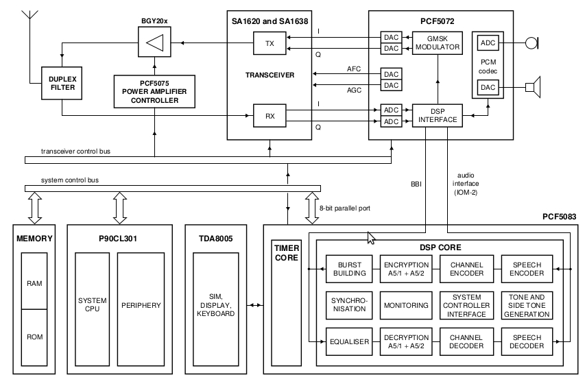
One of the largest documentation has GSM processor. I used GSM DSP to show that it really is a DSP.
8. PCF5083 processor from Philips: http: //pdf.datasheetcatalog.com/datasheet/philips/PCF5083.pdf
Over 100 pages get more information to radio amateurs that many have never not worked with it. If the GSM transceiver hams know many phenomena and can skip the explanations here reading must be done carefully.
External oscillator frequency uses are both 'classic' and 32 768 kHz GSM 13MHz time base.
But if we look in more detail the at controller and DSP communication, we see a lot of threads that should be "fired", ie the data bus and address bus.
D0..D7 and A0..A6 are 8 data wires and 7 for address data, making it difficult sticking together.
We note the description of the datasheet:
RX RF part 890-915MHz convert radio signals into a "complex baseband signal" consists of signal phase (I) and quadrature signal (Q). In the limit of -104 dBm , receiver has automatic gain control (AGC) and software controllable.
The I and Q signal reaches the audio codec PCF5072 (or PCF5073). In this IC I and Q signal is passed through A / D or D / A as appropriate (at 270KHz) with an accuracy of about 2x13biti.
Audio, sample is 13-bit uniform PCM format (114kbiti / second) is then compressed at 13kb / sec.
IC PCF5083 do:
- Compressing voice ("encryption / decryption" in accordance with A5 / 1 and A5 / 2).
A5 / 1 and A5 / 2 although often used in literature about them no public documentation.
-Frequency Correction Burst (FCB)
-Synchronization Burst (SCH)
-Monitoring BCCH, monitoring STIs nearby
-Coding / Decoding channel. Here is more detail to take effect at all.
Time required for a burst TDMA can be programmed with an accuracy of a quarter of a bit (1 / 500TDMA).
PCF5083 has two clock signals: 13 MHz, mainly used for the calculation of TDMA time, and that the internal PLL reference clock.
Secondary Clock 32.768 kHz is used for clock, calendar, Watchdog Timer and Sleep reduction in some cases. Internal PLL can generates 13, 39 and 52 MHz
To continue to clarify concepts I will also refer to Net Monitor from Siemens. Also for an old phone :
http://www.gasbag.wz.cz/mon/monxx.html
In GSM 900 we have channels 1-124 (extended in 1024).
To calculate the starting frequency channel number used to have:
The lowest frequency + 0.2 MHz (space between channels) *Xn (channel number).
For example downlink we have f = 935 MHz + 0.2 MHz *Xn
We thus for a pair duplex communication channel -TX Rx channels, or, in other words, a pair uplink downlink. In GSM900 frequency band between emission and the reception there is a "distance" of 45MHz.
I'll just put these lists beginning to emerge anyway from calculation:
(ARFCN = Absolute radio-frequency channel number)
Channel: 0, Band: EGSM-900 Uplink: 890 MHz Downlink: 935 MHz
Channel: 1 Band: GSM 900 Uplink: 890.2 MHz, Downlink: 935.2 MHz
Channel: 2, Band: GSM 900 Uplink: 890.4 MHz, Downlink: 935.4 MHz
Channel: 3 Band: GSM 900 Uplink: 890.6 MHz, Downlink: 935.6 MHz
Channel: 4, Band: GSM 900 Uplink: 890.8 MHz, Downlink: 935.8 MHz
Channel 5, Band: GSM 900 Uplink: 891 MHz Downlink: 936 MHz
... ...........
Channel: 124; Band: GSM 900 Uplink: 914.8 MHz, Downlink: 959.8 MHz
extended to:
Channel: 1023 Drinking: EGSM-900 Uplink: 889.8 MHz, Downlink: 934.8 MHz
Frequency vary considerably depending on the standard GSM900: E-GSM, P-GSM, GSM-R. In all three the difference between radio channel and the receive channel is 45MHz.
Net Monitor goes by different names depending on the phone manufacturer. The best known is that of Nokia.
Only certain phone models have Net Monitor and in other cases only certain SIM cards allow telephone operators Net Monitor activation. The list of phones that support Net Monitor and activation mode is very long and will not be discussed here. I can say that Ericsson has one of the worst NET Monitor information.
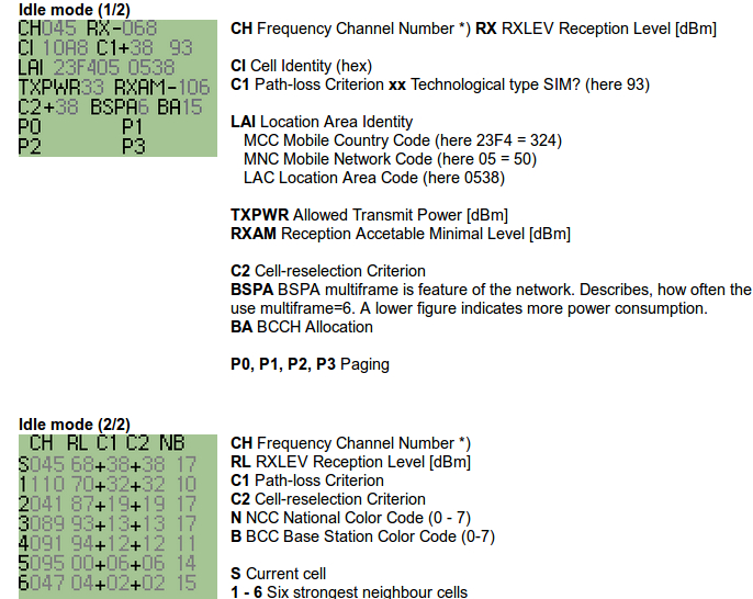
Thus using this menu that we have: assigned channel frequency, the reception cell identity, maximum emission level, selection criterion cell, BCCH allocation.
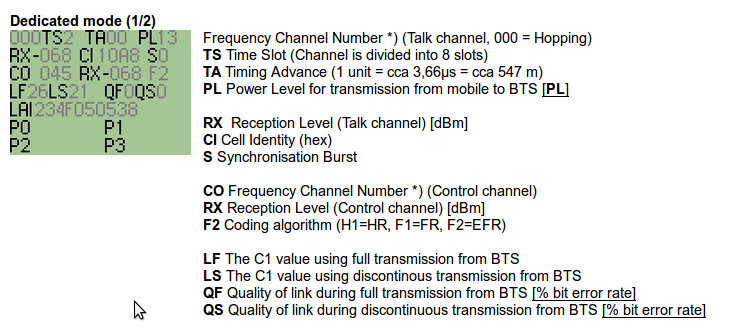
In dedicated mode, ie when making a call, the phone displays additional: Time-slot (1 of 8) Time advance ( packet should be sent in advance to take his time slot. It depends on the distance phone-BTS, 1unit = approx 3,66us = approx 550m) and next 6 or 12 BTSs that could be selected in order. For each BTS is shown reception level and other characteristics.
AT Commands for managing radio interface:
AT with response AT OK - the phone supports AT commands.
Most phones tested using asynchronous serial protocol 9600N1 (9600b / s, no parity and one stop bit, one start bit). To check the serial line when in Idle must have + 5V or + 3.3V appropriate. "Fall" in home 0V is indication of start bit. Many phones "guess" baud-rate used.
AT + CSQ - quality signal reception. Returns a reception power indication (0..31 = under -113dBm ...- 51dBm or over). Command that most phones supports.
You'll probably it is exaggerating when switching from dBm to remind W size that I'm used when talking transmit power at least.
Power transmission and reception level W is more suggestive. Although these differences in power between signal transmission and reception, or will be used in physics notation P = 1E-9W which is quite unusual in electronic. A logarithmic scale is used to include the power transmission and reception in an understandable way.
http://www.bitweenie.com/wp-content/uploads/2013/03/dBm-to-Watts-equation.jpg
The bandwidth, quality factor, is "caculated" at 3dB below the maximum. Usual for me was simple: approx. 70% of the maximum.
Another way to understand at an acceptable level for software reverse engineering practice is Open BTS.
8. PCF5083 processor from Philips: http: //pdf.datasheetcatalog.com/datasheet/philips/PCF5083.pdf
Over 100 pages get more information to radio amateurs that many have never not worked with it. If the GSM transceiver hams know many phenomena and can skip the explanations here reading must be done carefully.
External oscillator frequency uses are both 'classic' and 32 768 kHz GSM 13MHz time base.
But if we look in more detail the at controller and DSP communication, we see a lot of threads that should be "fired", ie the data bus and address bus.
D0..D7 and A0..A6 are 8 data wires and 7 for address data, making it difficult sticking together.
We note the description of the datasheet:
RX RF part 890-915MHz convert radio signals into a "complex baseband signal" consists of signal phase (I) and quadrature signal (Q). In the limit of -104 dBm , receiver has automatic gain control (AGC) and software controllable.
The I and Q signal reaches the audio codec PCF5072 (or PCF5073). In this IC I and Q signal is passed through A / D or D / A as appropriate (at 270KHz) with an accuracy of about 2x13biti.
Audio, sample is 13-bit uniform PCM format (114kbiti / second) is then compressed at 13kb / sec.
IC PCF5083 do:
- Compressing voice ("encryption / decryption" in accordance with A5 / 1 and A5 / 2).
A5 / 1 and A5 / 2 although often used in literature about them no public documentation.
-Frequency Correction Burst (FCB)
-Synchronization Burst (SCH)
-Monitoring BCCH, monitoring STIs nearby
-Coding / Decoding channel. Here is more detail to take effect at all.
Time required for a burst TDMA can be programmed with an accuracy of a quarter of a bit (1 / 500TDMA).
PCF5083 has two clock signals: 13 MHz, mainly used for the calculation of TDMA time, and that the internal PLL reference clock.
Secondary Clock 32.768 kHz is used for clock, calendar, Watchdog Timer and Sleep reduction in some cases. Internal PLL can generates 13, 39 and 52 MHz
To continue to clarify concepts I will also refer to Net Monitor from Siemens. Also for an old phone :
http://www.gasbag.wz.cz/mon/monxx.html
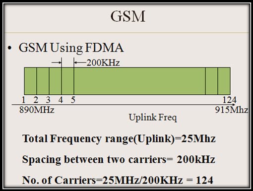
In GSM 900 we have channels 1-124 (extended in 1024).
To calculate the starting frequency channel number used to have:
The lowest frequency + 0.2 MHz (space between channels) *Xn (channel number).
For example downlink we have f = 935 MHz + 0.2 MHz *Xn
We thus for a pair duplex communication channel -TX Rx channels, or, in other words, a pair uplink downlink. In GSM900 frequency band between emission and the reception there is a "distance" of 45MHz.
I'll just put these lists beginning to emerge anyway from calculation:
(ARFCN = Absolute radio-frequency channel number)
Channel: 0, Band: EGSM-900 Uplink: 890 MHz Downlink: 935 MHz
Channel: 1 Band: GSM 900 Uplink: 890.2 MHz, Downlink: 935.2 MHz
Channel: 2, Band: GSM 900 Uplink: 890.4 MHz, Downlink: 935.4 MHz
Channel: 3 Band: GSM 900 Uplink: 890.6 MHz, Downlink: 935.6 MHz
Channel: 4, Band: GSM 900 Uplink: 890.8 MHz, Downlink: 935.8 MHz
Channel 5, Band: GSM 900 Uplink: 891 MHz Downlink: 936 MHz
... ...........
Channel: 124; Band: GSM 900 Uplink: 914.8 MHz, Downlink: 959.8 MHz
extended to:
Channel: 1023 Drinking: EGSM-900 Uplink: 889.8 MHz, Downlink: 934.8 MHz
Frequency vary considerably depending on the standard GSM900: E-GSM, P-GSM, GSM-R. In all three the difference between radio channel and the receive channel is 45MHz.
Net Monitor goes by different names depending on the phone manufacturer. The best known is that of Nokia.
Only certain phone models have Net Monitor and in other cases only certain SIM cards allow telephone operators Net Monitor activation. The list of phones that support Net Monitor and activation mode is very long and will not be discussed here. I can say that Ericsson has one of the worst NET Monitor information.
Thus using this menu that we have: assigned channel frequency, the reception cell identity, maximum emission level, selection criterion cell, BCCH allocation.
In dedicated mode, ie when making a call, the phone displays additional: Time-slot (1 of 8) Time advance ( packet should be sent in advance to take his time slot. It depends on the distance phone-BTS, 1unit = approx 3,66us = approx 550m) and next 6 or 12 BTSs that could be selected in order. For each BTS is shown reception level and other characteristics.
AT Commands for managing radio interface:
AT with response AT OK - the phone supports AT commands.
Most phones tested using asynchronous serial protocol 9600N1 (9600b / s, no parity and one stop bit, one start bit). To check the serial line when in Idle must have + 5V or + 3.3V appropriate. "Fall" in home 0V is indication of start bit. Many phones "guess" baud-rate used.
AT + CSQ - quality signal reception. Returns a reception power indication (0..31 = under -113dBm ...- 51dBm or over). Command that most phones supports.
You'll probably it is exaggerating when switching from dBm to remind W size that I'm used when talking transmit power at least.
Power transmission and reception level W is more suggestive. Although these differences in power between signal transmission and reception, or will be used in physics notation P = 1E-9W which is quite unusual in electronic. A logarithmic scale is used to include the power transmission and reception in an understandable way.
http://www.bitweenie.com/wp-content/uploads/2013/03/dBm-to-Watts-equation.jpg
The bandwidth, quality factor, is "caculated" at 3dB below the maximum. Usual for me was simple: approx. 70% of the maximum.
Another way to understand at an acceptable level for software reverse engineering practice is Open BTS.

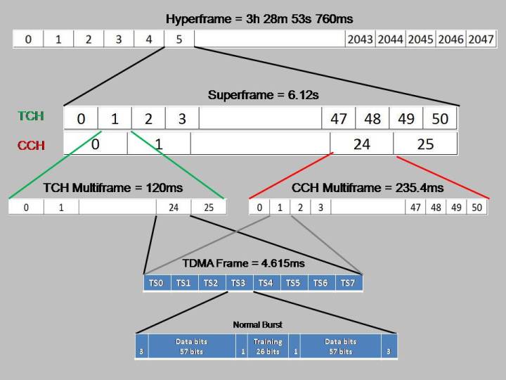
In a TDMA frame........
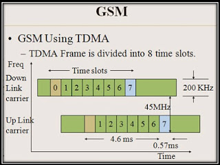
After dividing the 900MHz band in multichannel receiver and multichannel broadcasting (FDMA), time division's time in several channels (TDMA).
FDMA:
http://4.bp.blogspot.com/-kjgzMUuRweY/T14cXxGELhI/AAAAAAAAAGA/jlobC3HId44/s1600/gsm_fdm.bmp
A detailed hiperframe:
http://gnuradio.org/redmine/projects/gnuradio/wiki/OpenBTSTime_Division_Multiple_Access_%28TDMA%29/2
Each frequency channel is divided into eight time slots marked 0..7. GSM operating in full duplex. A communication channel is associated with a pair of frequencies: uplink and downlink. The channels are spaced 200KHz (see ARFCN, Absolute Radio Frequency Channel Number).
A time slot is 576.9 microseconds.
Date burst. A TDMA frame can be:
- Normal- Burst (NB) - sequence "normal" in which information is transmitted (with training bits in the middle and tail bits in margins)
-Frequency Correction Burst (FB) - correction channel allocated by the BTS
-Synchronization Burst (SB). It allocates TDMA Frame Number (FN) and Base Station Identity Code (BSIC)
-Access Burst (AB) access "random" and compensation. Used for correction Timing Advance.
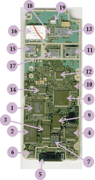
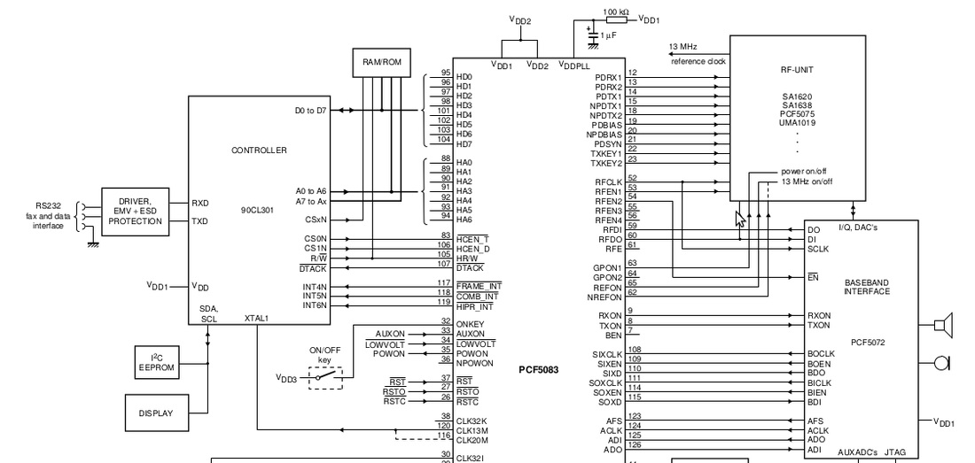
P90CL301BFH - board micro controller at this phone
Datasheet you find at www.datasheetcatalog.com
http://www.datasheetcatalog.com/datasheets_pdf/P/9/0/C/P90CL301BFH.shtml
Note VDD1..3 + poweer. The controller is 4x20 pin, 80-pin, that to be easier to count pins. The pins are numbered starting with pin number 1 in the counterclockwise. Thus VDD3 = pin 10 , VDD2 = pin32 (pin20 + 12) and VDD1 = 69 pin (pin12 in the reverse trigonometric from pin 1). We also have VDDA pin 59 now neglected.
It will be measured the voltage on these pins to evaluate the "height" serial signal.
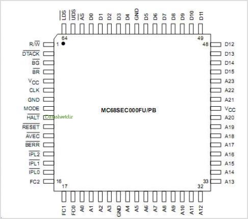
MC68000 controller is compatible with Motorola 68K writing or otherwise.
Projects of 68k (with source citation):
http://s100computers.com/My%20System%20Pages/68000%20Board/V2%2068K%20CPU%20Board.jpg
http://circuits.datasheetdir.com/265/M68000-pinout.jpg
http://www.classiccmp.org/cini/images/ht68k-lg.jpg
http://www.classiccmp.org/cini/ht68k.htm
http://info-coach.fr/atari/hardware/STE-HW.php
I know this is about Atari, another topic, another 'junk'. Who is interested can give search with 'Atari computer'
Finally there is a forum for this controller:
http://www.easy68k.com/EASy68Kforum/index.php
After reading them, if we take into account the difficulty of finding documentation on 'flashing Philips Diga' should be renounced to program this controller.
Controller is old, but very good, 16-bit. It controls the rest of the modules on the board: GSM processor (DSP GSM), VCO in PLL IC, radio transceiver, A / D converter, emission power controller.
GSM Signal Processing DSP should be a fast, qualities microcontroller. It will be used 13MHz quartz, time base for GSM. Open BTS uses 56MHz quartz, which are 13MHz multiplied.
We use a controller Microchip dsPIC probably one that has a clock to 120MHz, 30M instructions / second.
The following reasons:
- there is documentation
- most hobbyists use Microchip in detriment of Atmel microcontrollers
- can be easily programmer (I'll use a PICKIT 2)
You should have a logic analyzer or an oscilloscope (preferably digital), wich I do not possess. But the "fireworks" should be measured on a maximum speed serial communication bus.
Test: tester meter that use a sewing needle! Yes, a sewing needle!
How to solder? :
The safest would be solder on pins integratelor. We will not risk exfoliation of PCB. If there is a SMD codensator that you can solder ... it's not too hard!
Controller for keyboard / LCD
DA8005AH29 (TDA8005AG product Phiplips)
http://pdf.datasheetcatalog.com/datasheet/philips/TDA8005AG.pdf
In other cases occurs with another name, which may induce somewhat in error eg OM5199H
http://www.kanda.com/blog/programming/smart-cards-smart-card-programmer/
http://www.overunity.org.uk/picprogsdk/whatcard/index.htm
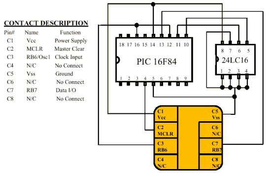
SIM card is a combination of PIC16F84 and a memory 24C ... Most SIM cards can not be rewritten (have PIC16C ... without refer to the numbers, calendar, ... which is stored in the memory 24C ....)
There are Gold Card SIMs that can be rewritten.
For example, a $ 4 GOLD card:
http://store.comet.srl.ro/Catalogue/Product/4084/
What is of interest here is the reading old SIM cards that can not be opened for recovering your phone numbers in the phonebook.
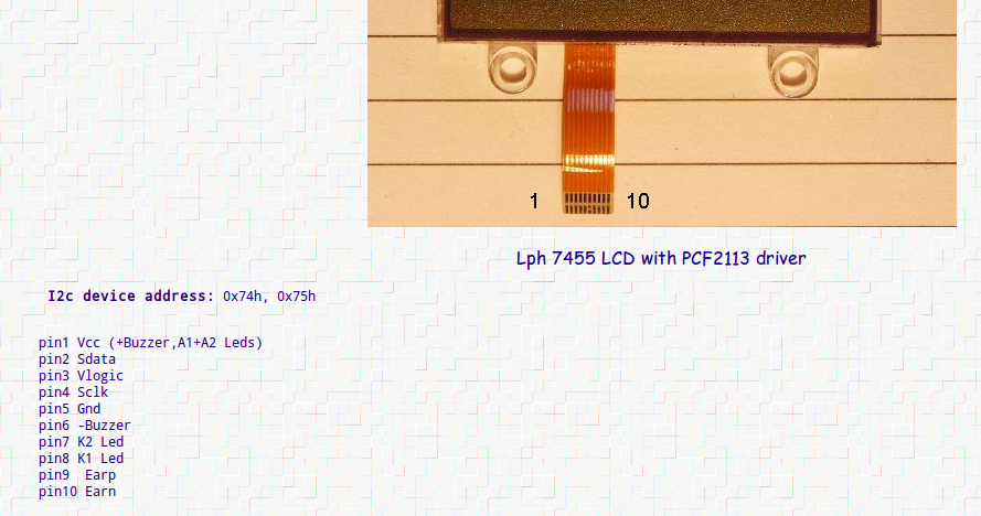
About LCD is very bad, most LCDs in such phones have "fallen" lines. However I note configuration pins and LCD controller:
http://www.module.ro/siemens_lcd.html
A typical application of DA8005AH.
Memoirs:
I 29LV400T-120E, IC near microcontrller, "USB memory stick"
http://pdf.datasheetcatalog.com/datasheets/560/175578_DS.pdf
4Mb (mega bits) CMOS 3V.
D43256BGW-A12X-9JL (UPD43256BGW-A12X-9JL produced by NEC). Two other smaller IC near the controller.
http://pdf.datasheetcatalog.com/datasheet2/f/0xogkcrrt5071aqz7txh3usootpy.pdf
32KB Static RAM
This controller will not be ignored, but should be considered separately from the rest of the modules.
Image from:
http: //inside-gsm.nărod.ru/component_side_description_dig.html
(this image can be found on Softpedia )
Were discussed:
1.microcontrollerul, 2. Flash memory AM29LV400T, 256k16, 9. 3. And 2xSRAM NEC D43256BGW 32k8, volatile memory, 4. SIM reader, keyboard
Sldering the pin is very difficult, ideally interrupted route.
But because I want to work as a technician in electronics I will slder those wires!
Datasheet you find at www.datasheetcatalog.com
http://www.datasheetcatalog.com/datasheets_pdf/P/9/0/C/P90CL301BFH.shtml
Note VDD1..3 + poweer. The controller is 4x20 pin, 80-pin, that to be easier to count pins. The pins are numbered starting with pin number 1 in the counterclockwise. Thus VDD3 = pin 10 , VDD2 = pin32 (pin20 + 12) and VDD1 = 69 pin (pin12 in the reverse trigonometric from pin 1). We also have VDDA pin 59 now neglected.
It will be measured the voltage on these pins to evaluate the "height" serial signal.
MC68000 controller is compatible with Motorola 68K writing or otherwise.
Projects of 68k (with source citation):
http://s100computers.com/My%20System%20Pages/68000%20Board/V2%2068K%20CPU%20Board.jpg
http://circuits.datasheetdir.com/265/M68000-pinout.jpg
http://www.classiccmp.org/cini/images/ht68k-lg.jpg
http://www.classiccmp.org/cini/ht68k.htm
http://info-coach.fr/atari/hardware/STE-HW.php
I know this is about Atari, another topic, another 'junk'. Who is interested can give search with 'Atari computer'
Finally there is a forum for this controller:
http://www.easy68k.com/EASy68Kforum/index.php
After reading them, if we take into account the difficulty of finding documentation on 'flashing Philips Diga' should be renounced to program this controller.
Controller is old, but very good, 16-bit. It controls the rest of the modules on the board: GSM processor (DSP GSM), VCO in PLL IC, radio transceiver, A / D converter, emission power controller.
GSM Signal Processing DSP should be a fast, qualities microcontroller. It will be used 13MHz quartz, time base for GSM. Open BTS uses 56MHz quartz, which are 13MHz multiplied.
We use a controller Microchip dsPIC probably one that has a clock to 120MHz, 30M instructions / second.
The following reasons:
- there is documentation
- most hobbyists use Microchip in detriment of Atmel microcontrollers
- can be easily programmer (I'll use a PICKIT 2)
You should have a logic analyzer or an oscilloscope (preferably digital), wich I do not possess. But the "fireworks" should be measured on a maximum speed serial communication bus.
Test: tester meter that use a sewing needle! Yes, a sewing needle!
How to solder? :
The safest would be solder on pins integratelor. We will not risk exfoliation of PCB. If there is a SMD codensator that you can solder ... it's not too hard!
Controller for keyboard / LCD
DA8005AH29 (TDA8005AG product Phiplips)
http://pdf.datasheetcatalog.com/datasheet/philips/TDA8005AG.pdf
In other cases occurs with another name, which may induce somewhat in error eg OM5199H
http://www.kanda.com/blog/programming/smart-cards-smart-card-programmer/
http://www.overunity.org.uk/picprogsdk/whatcard/index.htm
SIM card is a combination of PIC16F84 and a memory 24C ... Most SIM cards can not be rewritten (have PIC16C ... without refer to the numbers, calendar, ... which is stored in the memory 24C ....)
There are Gold Card SIMs that can be rewritten.
For example, a $ 4 GOLD card:
http://store.comet.srl.ro/Catalogue/Product/4084/
What is of interest here is the reading old SIM cards that can not be opened for recovering your phone numbers in the phonebook.
About LCD is very bad, most LCDs in such phones have "fallen" lines. However I note configuration pins and LCD controller:
http://www.module.ro/siemens_lcd.html
A typical application of DA8005AH.
Memoirs:
I 29LV400T-120E, IC near microcontrller, "USB memory stick"
http://pdf.datasheetcatalog.com/datasheets/560/175578_DS.pdf
4Mb (mega bits) CMOS 3V.
D43256BGW-A12X-9JL (UPD43256BGW-A12X-9JL produced by NEC). Two other smaller IC near the controller.
http://pdf.datasheetcatalog.com/datasheet2/f/0xogkcrrt5071aqz7txh3usootpy.pdf
32KB Static RAM
This controller will not be ignored, but should be considered separately from the rest of the modules.
Image from:
http: //inside-gsm.nărod.ru/component_side_description_dig.html
(this image can be found on Softpedia )
Were discussed:
1.microcontrollerul, 2. Flash memory AM29LV400T, 256k16, 9. 3. And 2xSRAM NEC D43256BGW 32k8, volatile memory, 4. SIM reader, keyboard
Sldering the pin is very difficult, ideally interrupted route.
But because I want to work as a technician in electronics I will slder those wires!